2019-10-29

2019-10-28 OrangeBot Mockup


>>>Mockup<<<


1Mechanical Structure Mockup

With the arrival of the motors, wheels, mounting brackets and hubs, the mechanical construction can begin.
Guiding principle for the construction is the MVP strategy, in which a minimal working version, a vertical slice is built first. Functionalities are added as testing of more basic functionalities is successful.
Objective is to build the minimal structure that demonstrate the mechanical layout of four independent traction wheel with the intended form factor to comply with the Pi Wars 2020 specifications.


2Specifications

Maximum Footprint Width x Length x Height
  • 225mm x 300mm x 370mm Core platform
  • 225mm x 400mm x 450mm With challenge specific attachments
  • 325mm x 500mm x 450mm With extensible flaps

Illustration 1: PiWars Size Specifications

2.1Motor Block Components

Component chosen for the Motor Block are:
Illustration 2: OrangeBot Motor Block Components

Illustration 3: OrangeBot Motor Block Mechanical Drawings
Both the Hub and the wheels needs to be modified to fit the motor block.


2.2Layout

OrangeBot is going to use four independent DC gearmotors with wheels. A central joint is going to allow the platform to swivel around the longitudinal axis of the robot.

Illustration 4: OrangeBot Motor Block Mechanical Drawings


3Mechanical Construction

This section details the manufacturing steps for the mechanical construction.

3.1Motor Block Assembly

First step is to modify the hub and the wheel to fit the motor block.
The motor 6mm shaft already fits the 6mm hub hole.
The wheel must be modified to fit the hub. This requires enlarging the central hole to 12mm.


Video 1: Enlarge wheel hole to 12mm

Next step is to drill through both the hub imperial satellite holes and the wheel to create three M3.5 through hole to fix the wheel to the hub.


Video 2: Satellite M3.5 satellite holes
This process is repeated for all four wheels.


3.2Robot Base MVP

The minimal workable base is a simple slice of acrylic cut to shape and drilled to host the four motor block assemblies. This MVP is meant to demonstrate the traction and electronics and allow to get a feel for the size, in preparation for the next step of the mechanical assembly.

3.2.1Cut Mask

First step is to design the cut mask to accommodate the four motor blocks. The encasing of the encoder of the gearmotors has been removed to save space and because the wirings of the gearmotors are going to be replaced altogether anyway.

Illustration 5: Base MVP Cut Mask


3.2.2Acrylic Sheet

For the sheet of acrylic, the upper plate of our previous robot 'Topolino' was used. The cut mask is kept in place by a few stripes of black tape.

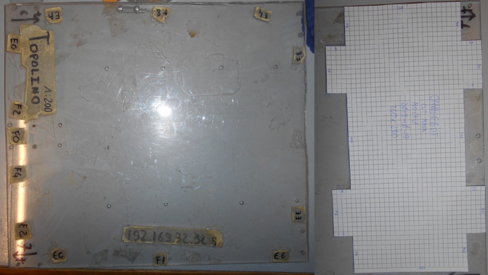
Illustration 6: Acrylic


3.2.3Cut Acrylic Sheet

Using a vertical saw, the acrylic is cut to shape.

Illustration 7: Cut acrylic


3.2.4Acrylic Robot Base

The result is the simplest possible support for the motors.

Illustration 8: Acrylic Robot Base


3.3Motor Mounting Brackets

Now the mounting brackets can be assembled on the robot base.

3.3.1Sanity Check Size

Check that motor block assemblies comply with the PiWars specifications with some margin.
Margin is an healthy 30 x 20 mm.

Illustration 9: Check Size


3.3.2Place Motor Brackets

Mpounting brackets for the motor are placed precisely along guide lines and held in place.

Illustration 10: Place Brackets


3.3.3M3 Drills

M3 holes are drilled as precisely as possible. M3 bolts are used to keep the bracket in place as new holes are drilled.

Illustration 11: Drill acrylic sheet


3.3.4Clean Drills

Clean up the holes and apply M3 bolts to keep brackets in place.

Illustration 12: Countersink and clean up holes


3.3.5Assembly Bracket

The brackets are all assembled and aligned. Now the motors can be attached as well.

Illustration 13: Assembly Motor Brackets


3.4Assembly Motor Blocks

With the mounting brackets and the motors assembled, now the hub wheel assembly can proceed.

Illustration 14: Motors Assembled


3.5Assembly Wheels

Order of assembly:
  1. Insert the M3 wheel screws in the hub (without the wheel)
  2. Insert the hub on the axle and tighten the hub-axle screws.
  3. Insert the wheel.
  4. Tighten the M3 bolt

Illustration 15: Wheel and Hub before and after Drill

Illustration 16: Before and After Drill
It's very tricky to tighten the M3 screws on the wheel.


4Skin Mockup

Cardboard plates were used to prototype the outer structure of the OrangeBot platform. M3x10 screws were used to bolt the plates together, resulting in a surprisingly solid and rigid structure.

Illustration 17: OrangeBot Mockup
The platform is modelled after an Armoured Personal Carrier or APC. The platform is going to feature a fully operational turret, tentatively equipped with an RC grade BB gun emplacement. Tentatively, the turret is going to achieve full 360° turn capabilities and +/-15° of azimuth. The camera is going to be mounted on the gun emplacement for targeting and navigation.

5Conclusions

This document detailed the development of the simplest possible vertical slice for the mechanical assembly.

Illustration 18: OrangeBot Mechanical MVP
ToDo list:
  • Thread the holes on the hub to M4 for ease of assembly
  • Design a base to accommodate the longitudinal joint
  • Design the turret and the chassis


2019-10-16

2019-10-13 AT4809 VNH7040 Test


>>>PiWars 2020 Page<<<


1Motor Driver Test

The objective is to build a Raspberry Pi Hat capable of controlling four DC motors.
A through research was conducted to select the right H Bridge component for the PiWars Hat.
The scope of this document is to detail the choice and test of the driver with the PiWars Motor.


1.1H Bridge Specifications

The H-Bridge driver must be small enough so that four of them can fit a Raspberry 2/3 Pi Hat. The minimum steady current of each driver must be 10A or above. The driver must be able to be powered by 3S or 4S LIPO batteries.
Nice to have are ultrasonic PWM, current and temperature sense, ease of soldering and ease of layout and cheap component.
Specifications:
  • 3S/4S LIPO : 10.2V to 14.8V
  • Current: 10A
  • Small footprint
  • Fully integrated: MOS +MOS drivers + control logic +sense circuitry
Desirable features:
  • High frequency PWM
  • Current Sense
  • Temperature Sense
  • Friendly layout
  • Easy to solder


2H Bridge Choice

The H-Bridge is the most important component of the board. A large number of H-Bridges from may manufacturers have been evaluated. Amongst the options were:
  1. IFX9201
  2. TLE7209
  3. VNH5019
  4. BTN7930
  5. BTN8982
  6. VNH7040
In the end the VNH7040 was selected as H-Bridge of choice.


Illustration 1: VNH7040 Block Schematics
With a current of 35A, a voltage of 28V and a PWM of 20KHz the VNH7040 met or exceed all desired specifications for the PiWars Hat.
This is a new component meant for automotive. ST was able to fit three dies, allowing for true power mosfet and the specifications of the components. The previously choosen H-Bridge for the HotBlack Shield was the BD62321 with just 3A of current.


2.1Features

The basic feature is the 20KHz PWM controls. A microcontroller PWM channel with a number of digital I/O are needed to select between various output configurations:
  • Open
  • Break (high and low)
  • Clockwise
  • Counter clockwise
The VNH7040 features all the standard integrated safety systems. Over current and over temperature.
More interesting, the VNH7040 features a single current output sense channel whose function can be selected by an internal multiplexer by a number of digital I/O. Current, temperature and even supply voltage are all monitored. Being a current output allow to minimize the noise due to differences in the 0V common rail.
The sense pin also report faults of the internal safeties that can be reset.
With the VNH7040, current PID , temperature and voltage monitoring.


2.2Interface

Interface with the microcontroller requires a number of pins.

Illustration 2: VNH7040 Truth Table
The truth table is very rich, requiring 5 digital output one PWM channel and one ADC current channel.
By carefully sorting the pin for the four drivers, two available pin configuration emerge.

Illustration 3: VNH7040 Pin Allocations
Option 1 connects the VNH7040 PWM pin to the microcontroller PWM channel. It leaves the motor open during the low PWM time, letting the current flow through the recirculation diodes. This option opens the possibility of using an external diode to bring some losses outside the driver itself.
Option 2 connects the VNH7040 INB pin to the microcontroller PWM channel. This makes the motor break during the low PWM which is a more efficient and forceful drive settings. In this option the meaning of the pins is more straightforward with a DIR and ENABLE pin.
In both options, INA and SEL0 can be connected to the same logic pin to save one microcontroller pins for each driver.
In both options, SEL1 and MSENSE_ENABLE can be shared between all four drivers.
Currently Option 1 has been tested.


3Test VNH7040

3.1Setup


Illustration 4: Setup
Controls are generated by the AT4809 curiosity nano kit from microchip. It's the same microcontroller that will power for the PiWars Hat.
Programmer is the Atmel ICE using the UPDI program and debug interface.
Programming IDE is the AVR Studio 7
One driver has been connected in OPTION 1 wring.


3.2Firmware

The firmware uses the same modules intended for use in the PiWars hat.
The RTC provides a periodic interrupt at 1KHz to orchestrate the PWM slope generator and the LEDs.
The powerful timer type A is used in split mode to generate up to 6 channels of single slope PWM at 80KHz. It's configured to generate four independent 20KHz 8bit single slope PWM channels.
Control signals are fed to the VNH7040 evaluation board to test the driver in both directions.

Illustration 5: Firmware Architecture
>>>AT4809 VNH7040 Test Firmware repository<<<

3.3Test

The test is a success. The hardware chosen to drive the PiWars motor block works as intended.

Video 1: AT4809 VNH7040 Test


4Conclusions

This test served as validation for the AT4809 and the VNH7040 components. Design of the PCB can proceed.
The scope of the PiWars hat is ambitious, with four speed and current PID running concurrently on a single AT4809.
Quad quadrature encoder acquisition is yet to be tested.
Current sensing capability of the VNH7040 is yet to be tested.


2019-10-08

2019-10-05 SoW-B Remote Control

>>>Seeker Of Ways B<<<


>>>Seeker Of Ways B: Remote Control Demo<<<


1SoW-B Remote Control MVP

Previous test of the board demonstrated that the HotBlack Shield V1 and the Raspberry Pi are working as intended.
Next steps are:
  • Serial Interface: Test bidirectional data transfer between RPI and HotBlack Shield V1
  • Firmware: Running on HotBlack Shield V1. Port from servomotors to DC motors. Bugfix.
  • Software: Running on the RPI. Change OS image name. Test webserver and remote control.

2Software Upgrade

The operating system is a cloned flash image transplanted directly from Maze Runner to Seeker Of Ways B.
Two configurations needed to be updated:
  • IP Address: Ethernet. Changed to 192.168.1.203
  • Image Name: Changed to “Seeker Of Ways B”

Illustration 1: OS Robot Name


3Test: Serial Interface

In order to test the serial interface, two test modules have been implemented.
  • NODE.JS application that sends and receive data through the serial interface on the GPIO connector.
  • Added driver for the UART to the firmware running inside the shield. Implements loopback and send one character every second.
For the serial test, the NODE.JS application send the string “P” including the terminator two times a second, and print on the console every character received from the UART.
UNIPARSER V4 is the firmware library that decodes an incoming serial streams in commands and automatically call handler functions with arguments like you would do with a scanf.
The Firmware is configured to toggle LED0 each time a command is fully decoded . Valid commands for this test are:
  • “P” Pin command. Used to reset the communication timeout.
  • “F” Find command. The board answers with its signature “SeekerOfWaysB-00002”
  • “PWMR%SL%S” PWM command. Set the PWM of two DC motors to the 16 bit integer provided in input.

Illustration 2: Serial Test Architecture
Through a SSH client is possible to launch the NODE.JS application in execution and receive the console output.


Illustration 3: Serial Test SSH Console Output
The test was a success on first try with a baud rate settings of 56Kb/s.

Illustration 4: 56Kb/s AT644 UART0 TX channel waveform and decoding
With the success of the test, baud rate was increased to 256Kb/s on the RPI side and to 250Kb/s on the AT644 side. The mismatch is due to imperfection in the UART prescaler. Increasing the UART speed decreases the latency of the commands.

Illustration 5: 256Kb/s RPI ttyS0 TX channel waveform and decoding
The waveforms look clean enough and there seems to be no trouble with the UART channel transmission in both directions.


4Test: Motor Control

With the serial interface operational, next step was to test control of the motors from the NODE.JS application running inside the RaspberryPi through the PWM command.
The architecture remains pretty much the same as the previous test.


Illustration 6: Serial Test Architecture
Two additional features were developed for this test, both tested and working:
  • Communication timeout: If the Raspberry pi dies and communication ceases, the HotBlack Shield stops all motors. Without it the robot would keep executing the last valid command, aka running straight into a wall.
  • Slew Rate limiter: The actual command to the motors cannot vary by more than a user defined value in PWM units per second. This makes sure the robot cannot be reversed in directions in short intervals, avoiding damage to both the motor drivers and the motors themselves.


Video 1: PWM waveforms


Video 2: Motor test with commands generated by the RPI


4.1Uniparser V4 Bug

Testing revealed a bug within the uniparser v4 library.

Illustration 7: Uniparser V4 bug
The command “PWMR-127L127” is translated as R=-127 | L = -127 (wrong) instead of R=-127 | L = +127. This likely happens because the argument sign flag is not reset from previous argument if an explicit sign is not used. Workaround is to explicitly send the + sign with positive numbers.

5Test: Remote Control

The stack to allow SoW-B to be controlled remotely via browser was developed for the Maze Runner MVP DEMO. Only a change in baud rate from 56Kb/s to 256Kb/s and a modification of the DC motor PWM command were necessary to port the software to SoW-B.
This application does not make use of the video stream component as SoW-B uses a raspicam while MR used an USB camera. A redesign of the video streaming software stack was due for a redesign anyway since the current pipeline only performs to about 300[ms] of latency.

Illustration 8: Seeker Of Ways B Remote Control MVP Architecture
The architecture of the remote control MVP demo works as intended. The test was made with a very slow slew rate limiting factor of 5.12[s]


Video 3: SoW-B Remote control MVP Demo
In this demo the wasd keys are bind to the direction of the platform.
Default PWM is 50% and can be increased/decreased with the +/- keys.


6Source Code Repositories

Link to the GitHub repositories for the NODE.JS application and the AtMega644A Firmware.

7Conclusions

The remote control of Seeker Of Ways B through a web browser is operational.
Next steps:
  • Install Wi-Fi access point functionality on the platform to allow control through web browser through Wi-Fi connection
  • Develop the Raspicam UDP WebRTC streaming pipeline
  • Fix Uniparser V4 issue
  • Add speed PID motor control on the PID


2019-10-04

2019-10-04 Ideal Diode


>>>Ideal Diode Page<<<


1Ideal Diode

1.1Problem

A common mistake is to connect the power wires of a board the wrong way, which powers the system with a negative voltage instead of the intended positive voltage.
The simplest protection against reverse voltage is a diode, but you are going to lose a lot of power due to the forward voltage.

1.2Solution

Instead of a simple diode, an ideal diode can be used to minimize conduction losses.


2Low Voltage Ideal Diode

The idea is to use a MOS switch instead of a simple diode. A simple bias circuit ensures that when input voltage is positive, the MOS switches ON and the forward diode is replaced by the ON resistance of the MOS sharply reducing forward losses.

Illustration 1: Low Voltage Ideal Diode Schematics
M_FW is the MOS that takes the place of the diode. A P-MOS with the source facing toward the output is the simplest solution. Putting the source on the other side means the source drain diode would let negative voltages through. Using a N-MOS would require a charge pump to generate the required gate voltage.
RPU makes sure M_FW is OFF in the default state.
M_INV is a signal transistor and what makes the bias network works. When VIN>0, M_INV switches ON dropping the gate of M_FW to 0V which is its ON condition.
RG is needed just to protect the gate of M_INV. There can be funky behaviour when there are harmonics at low voltage on the input, CF is there just to make a low pass filter and is optional.
When VIN<0 the source drain diode of M_FW is OFF and M_INV is OFF as well, meaning the output is disconnected from the input.


Illustration 2: Low Voltage Ideal Diode Waveform
The limitation of this circuit is that the gate-source breakdown voltage limits the maximum VIN to about 18V with typical MOS transistors.


3High Voltage Ideal Diode

If higher voltages are required, like 24V automotive, a different circuit is needed to protect the gates of the MOS switches.

3.1Zener

The simplest solution is to add a zener to the gate to protect it from big drive voltages.

Illustration 3: High Voltage Ideal Diode Schematics
Adding DZ1 means RS1 has to be added to limit the current flowing in M1 when DZ1 is active.
Having RS1 too low would limit response time and prevent the zener to activate. RS1 must guarantee the minimum zener current when the zener is supposed to switch on.
Another thing to consider is that now RS1 and RPU1 now form a voltage divider, meaning the gate voltage is reduced. This delay the switch on, but also lowers the maximum VGS. Depending on the application you might get away with just using resistors without zener diodes.
Now, this circuit has two MOS switches an the second MOS must also be protected by its own zener DZ2 with its own resistence to limit the zener current when DZ2 is on. The same considerations made for RS1 apply for RG1.


Illustration 4: High Voltage Ideal Diode Waveform
As can be seen fro the waveforms, the output behaves correctly, but this time the gate voltages are clipped to the zener diodes own zener voltage, making sure no component dies.


3.2BJT Version

One might think of replacing some or all of the MOS switches with BJT switches to avoid the gate breakdown voltage.
The original problem was that the diode had a forward junction voltage in series with the power line. Using a BJT in place of M_FW replaces a Vgamma with a VCEsat, not a big step up.
Bigger problem still is that BJT re vulnerable to reverse voltages on the BC junctions, typically limited to -5V before breakdown. Such conditions happens in this circuit when input voltage is negative.
In order for BJT to be used, a diode and a resistor have to be used to protect the BC junction from reverse bias. Not a big step up from using a zener, but doable.


Illustration 5: High Voltage Ideal Diode BJT Schematics
Same considerations apply for RG1 and RS1 as the previous circuit.


Illustration 6: High Voltage Ideal Diode BJT Waveform
Waveforms are mostly the same as before, except the BE junction is clipped to about 1V of dynamic.


3.3Current Mirror

Rather than protecting the base/gate of the lower switch, you can think about using a different bias circuit.
If you expose the emitter/source, the problem doesn't go away, but if you expose the collector/drain to the input voltage, you are keeping the GS/BE protected. Doing so requires an additional switch, forming a current mirror.
The Raspberry Pi uses a similar this approach, but it's not enough to protect the BE or the GS on its own. If you want to protect them from high voltages, you need a diode for each BJT and a zener/voltage divider for each power MOS.


Illustration 7: Low Side BJT Current Mirror


4External Control

Arrived to this point, since you have a voltage controlled diode you might think that by adding a control signal you can manually disconnect the power, achieving both reverse voltage protection and power disconnect functionality from the same MOS:
It doesn't work. If you disable the MOS with a positive input, its embedded diode is still there, and you are left with a diode instead of an ideal diode.
You cannot put the embedded power diode in reverse because it would let negative voltages through. You can only add another switch, which needs to be flipped in order to block positive voltages by default.


Illustration 8: Controlled Ideal Diode Schematics
M_EN is controlled by logic and can be used to disable the ideal diode. In this configuration, a positive enable will enable the diode, meaning the logic must be powered already.

Illustration 9: Controlled Ideal Diode Waveforms
The control logic must be independent from this protection anyway, or disabling it would power down the logic and that would disable the protection, leading to an oscillatory behaviour. This circuit is meant to protect power electronics independently from the logic in a controlled way.


5Improvements

I felt one could do better with the protection of the input MOS, and the solution was simple enough.

5.1Remove one component

You can remove the auxiliary MOS altogether.
The reason this works, is because the forward diode let voltage through allowing the divider RPU RPD to establish a VGS and switch the forward MOS on.
Illustration 10: Simplified Ideal Diode Schematics
The waveforms are the same as previous circuits.

Illustration 11: Simplified Ideal Diode Waveforms
Again, the zener can be omitted from the circuit depending on the voltage divider and response time required, but at least with this circuit you just need one zener.


5.2PTC

Since you went through the trouble of using an ideal diode, you probably want a fuse as well for good measure. A PTC resistor is convenient because it reset itself when it cools down.
One idea you might have, is to put the fuse in a spot where it can lower the GS voltage as it gets hotter, improving the response of the fuse, and leaving the forward MOS bear some of the heat as it get less switched on.
Illustration 12: Ideal Diode with PTC Schematics
It works. When the PTC is tripped by heat, its resistance increases, robbing voltage to VGS and lowering current even more.

Illustration 13: Ideal Diode with PTC Waveforms
There is one caveat, as M_FW takes some of the burden, PTC dissipates less heat, which might result in increased blocking current. Worst case scenario, the PTC trips faster, but settles at an higher overall blocking current.


5.3Lower Startup Threshold

Having added a PTC and removed one component, one might thing of trying to lower the startup voltage of the ideal diode by adding a switch as pull down network, but sharing the protection of the forward MOS.


Illustration 14: Low Activation Threshold Ideal Diode with PTC Schematics
It works. The low side MOS has to be an N type with SD replacing the pull down network of the forward switch. Now, the pull down resistor has just the job of bias and current limiting for the zener, and can be placed either at the source or at the drain of M1.
Putting it downstream is the obvious choice, and it behave as one might think.
If you put RPD2 upstream, something magic happen. Now, RPD2 forms a positive feedback loop with M1 in which more current, means more VGS which means more current.
Thanks to this effect, you can remove RPD1 from Gpwr to ground, because the leakage voltage of M1 is enough to get amplified into a fully switched on pull down MOS.


Illustration 15: Low Activation Threshold Ideal Diode with PTC Waveform
With this MOS, the threshold voltage at which the ideal diode switches on is lowered from 3.94V to 1.6V, this circuit retains all the protections and feature of the previous optimized circuit.


5.4Enable

The next idea is to add now an enable signal.


Illustration 16: Low Activation Threshold Ideal Diode with PTC with Enable Schematics
An enable MOS is added in series to disable the ideal diode. The protection works for all switches.


Illustration 17: Low Activation Threshold Ideal Diode with PTC And Enable Waveform
An idea can be to draw the logic power from the FW node, this way the low power logic can be powered even while not taking advantage of the saving of the ideal diode.
When the enable signal is sent, the power electronics is powered and the ideal diode activates